INDUSTRIAL JP
idstr.jp open shareJune 14, 2019
AT-10
nikko
interview
Artisanship for quality and consistency
// nikko interview
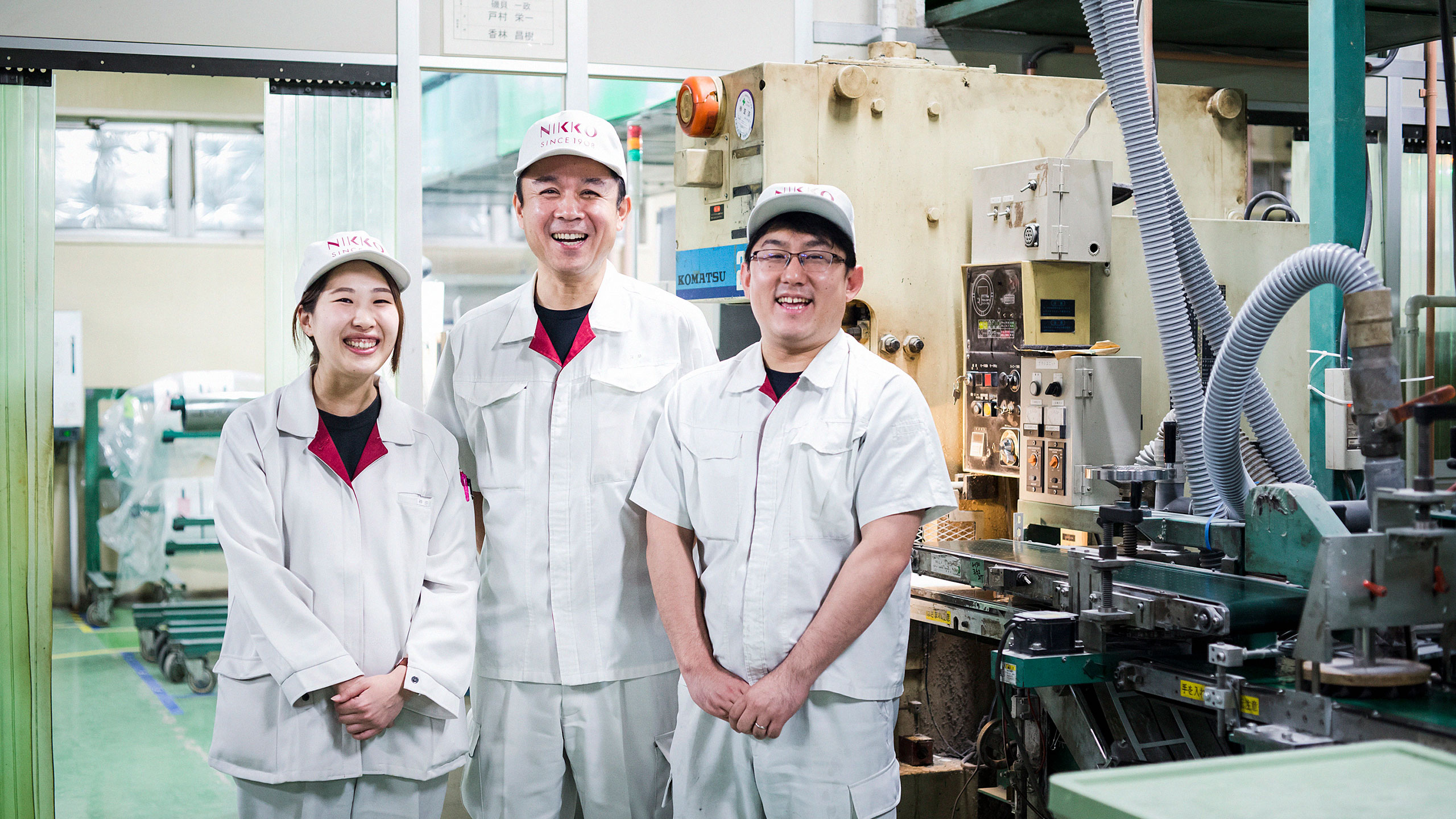
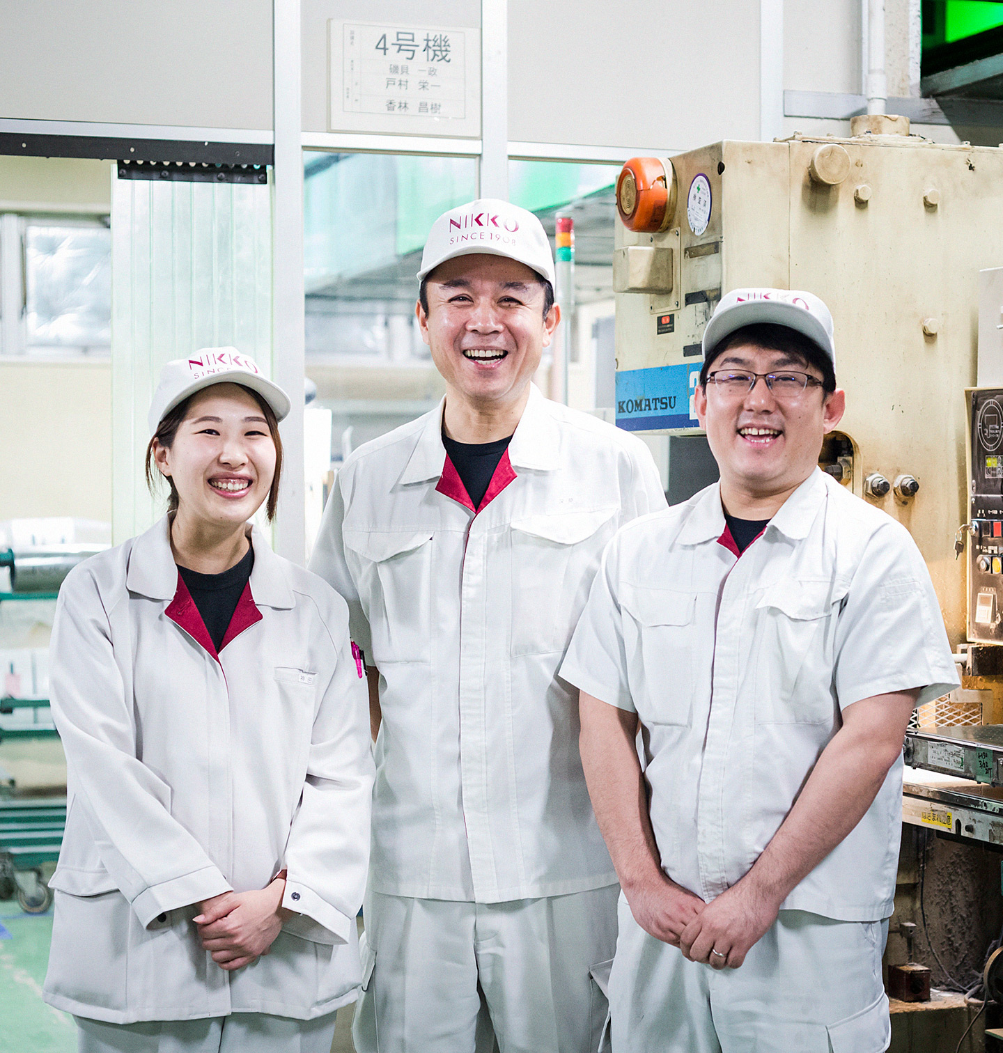
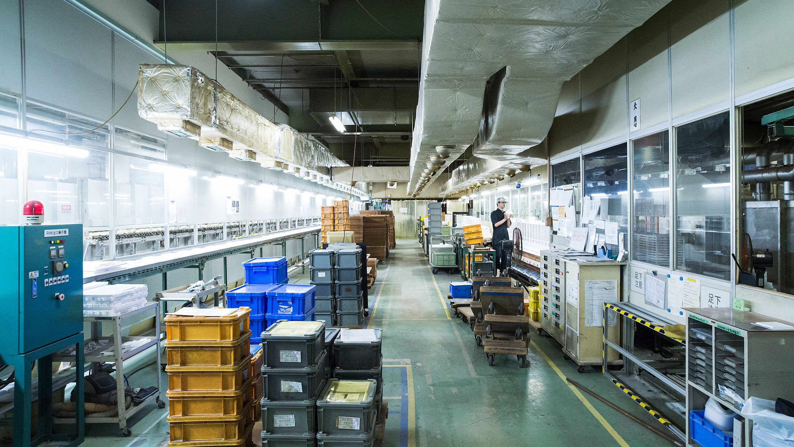
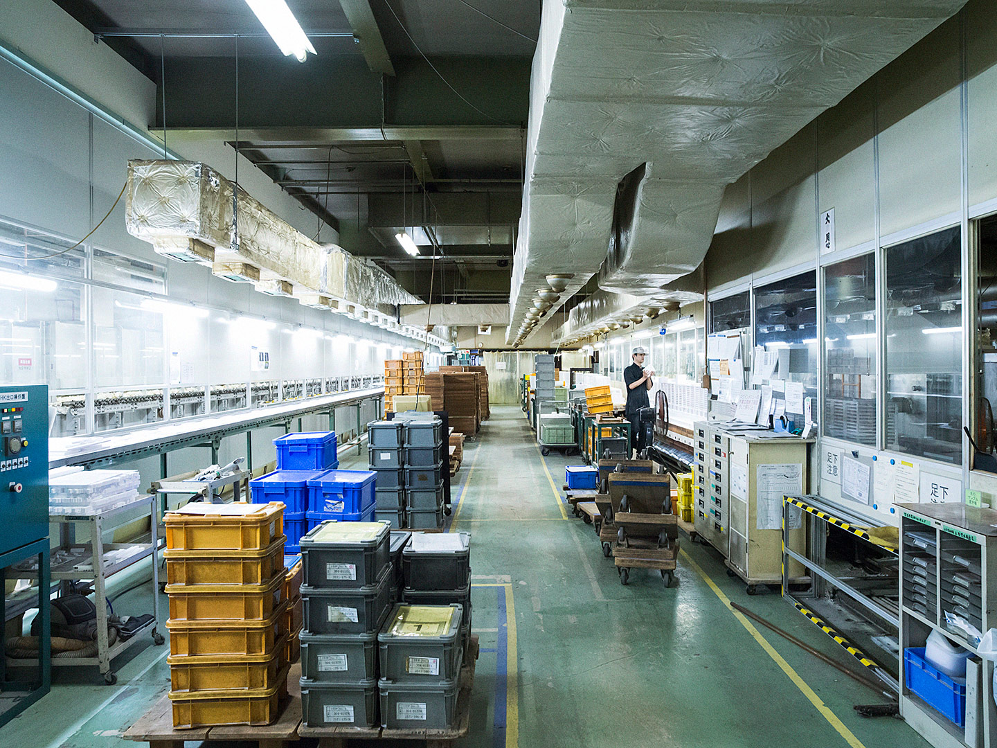
A few stops past Kanazawa station in Ishikawa Prefecture stands Nikko’s Hakusan factory. Founded during the Meiji era as a ceramics manufacturer, this time-honored company now manufactures electrical devices. We spoke to three workers at the factory. Century-old ceramics manufacturer Nikko Ceramics now makes electrical devices. We spoke to workers at their Ishikawa factory.
nikko ceramics
ID-10
nikko
foodman
The company started as a manufacturer of dishes and other ceramics. Business expanded from there, and today we manufacture circuit panels.
Up to now, INDUSTRIAL JP has focused on the manufacturing processes of factories that output metal products in shades of silver and black, so the flowing white materials in our video of Nikko’s factory certainly make an impression.
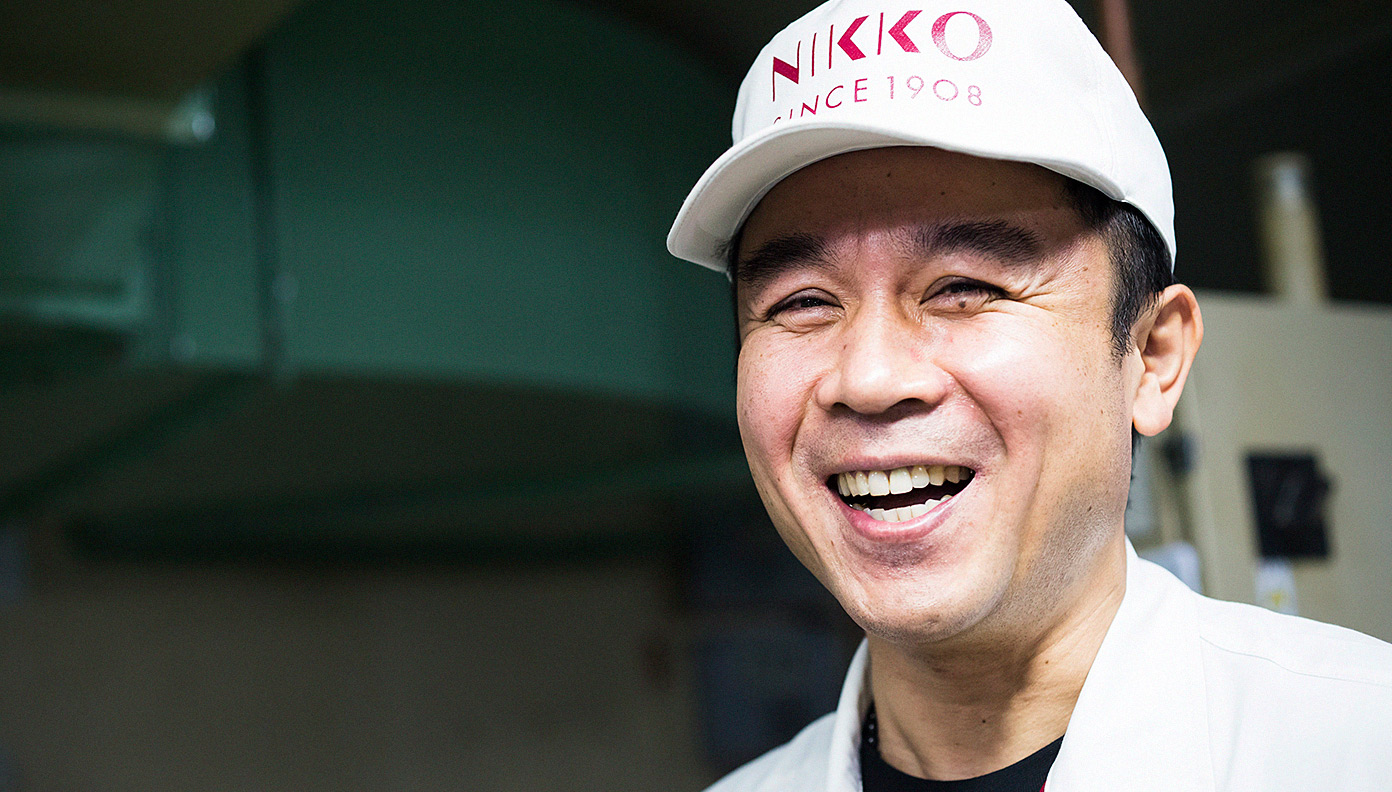
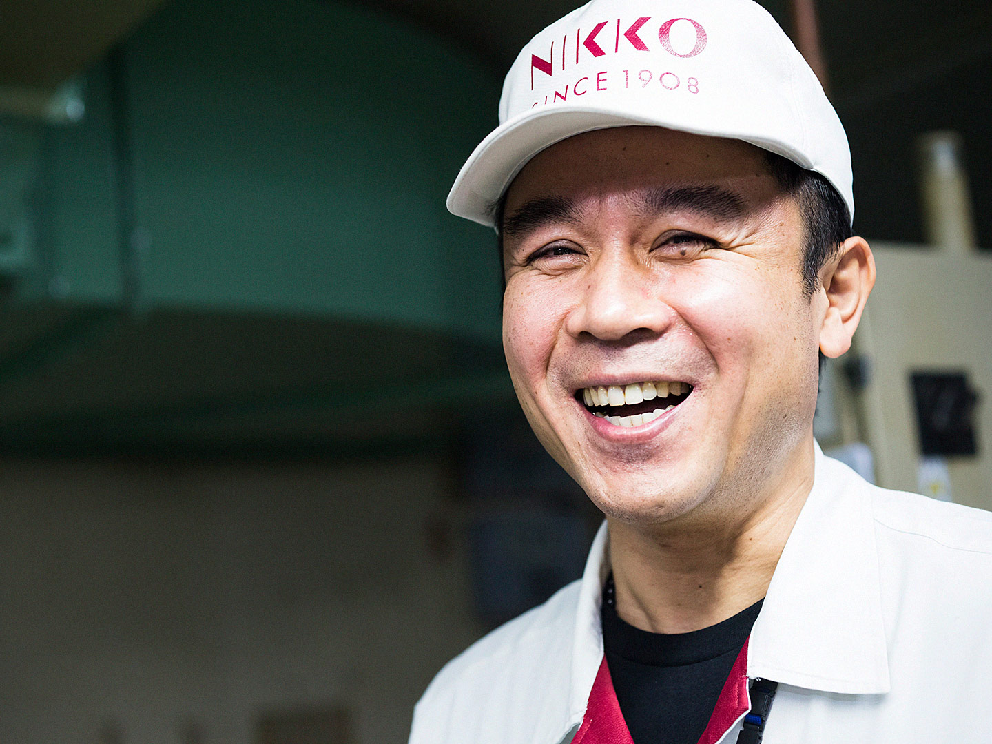
Fukakusa: This year marks the 111th year since Nikko’s founding, when the company started as a manufacturer of dishware and other ceramic goods. White dishware. The business expanded from there, and today we manufacture the “functional ceramics” that appear in the video, which are for use in electrical devices. Like for automobiles or office automation equipment, or controls for running equipment and machines. Basically circuit panels.
Going from dishes to circuit panels seems like quite a leap (laughs).
Fukakusa: I suppose it does (laughs).
“Circuit panels” makes me picture a green panel with gold lines all over it. Is that what you mean?
Fukakusa: Green panels are made of plastic, but here at Nikko we make ceramic panels.
I see. So those white panels are ceramic, then. How are ceramic panels different from plastic panels?
Fukakusa: The end use is different. In cars, for example. It gets very hot around the engine, so the panels need to be heat resistant. Or in the case of an electric substrate, the part itself may produce heat. Ceramics are better for heat resistance and heat dissipation than plastic. So “heat” is the key word here.
We make electrical parts, but the manufacturing process still has some quite analog aspects. It’s similar to baking a cookie (laughs).
What is the flow of your manufacturing process?
Fukakusa: We start by blending powdered ceramic material. The main component is called alumina, an oxidated aluminum material. The strength of the finished ceramic depends on how the material is mixed, so we adjust the mix according to the product. Then we form the material into thin, soft sheets.
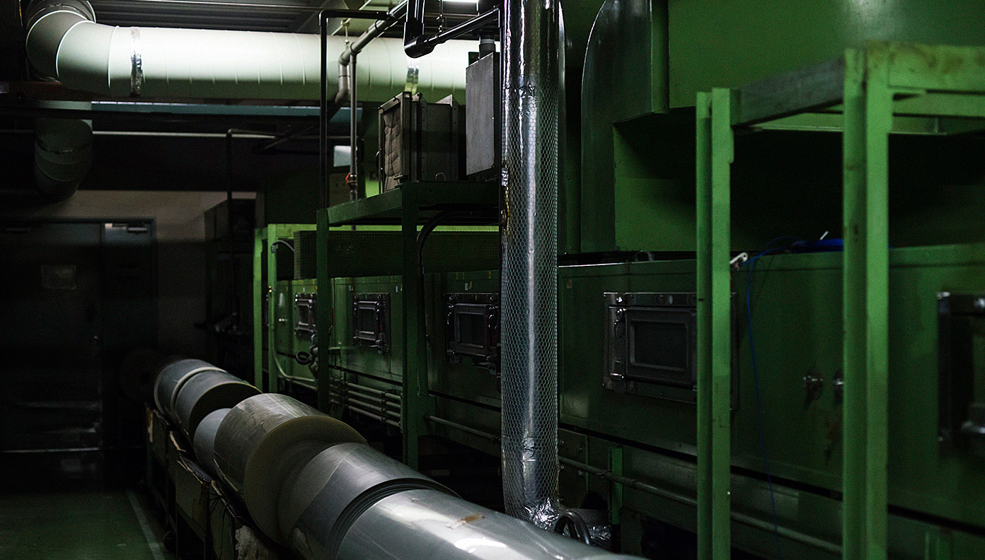
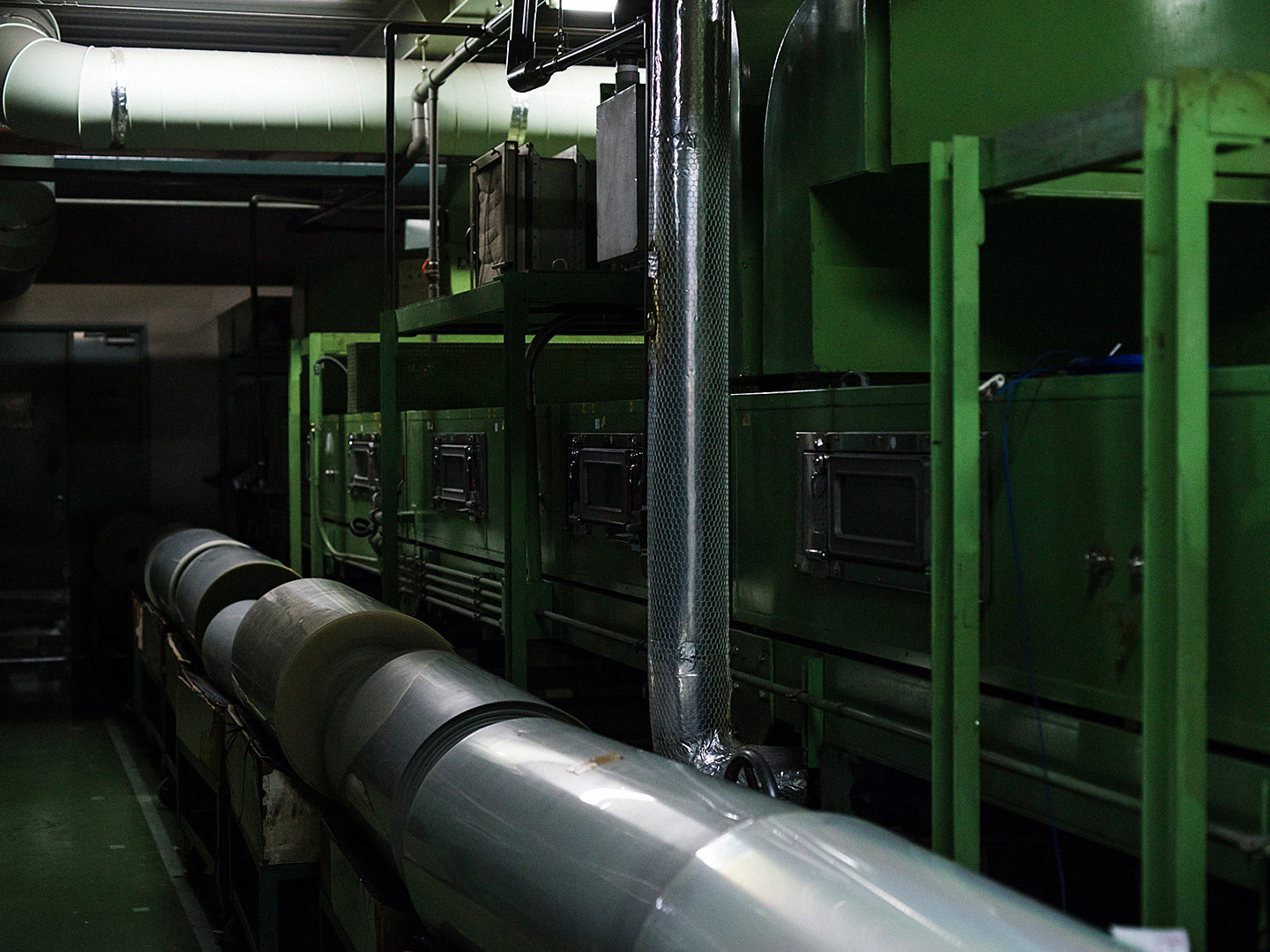
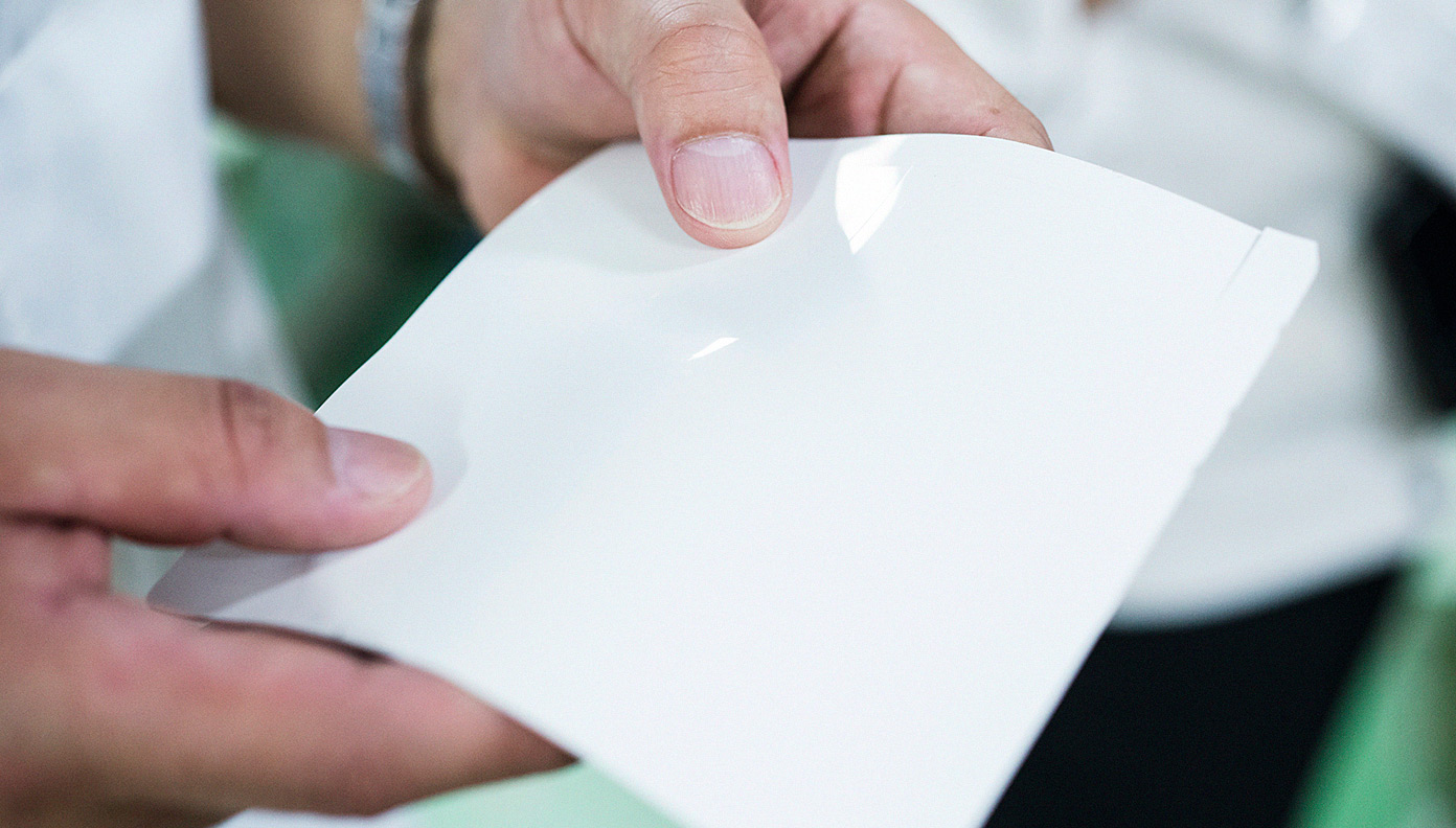
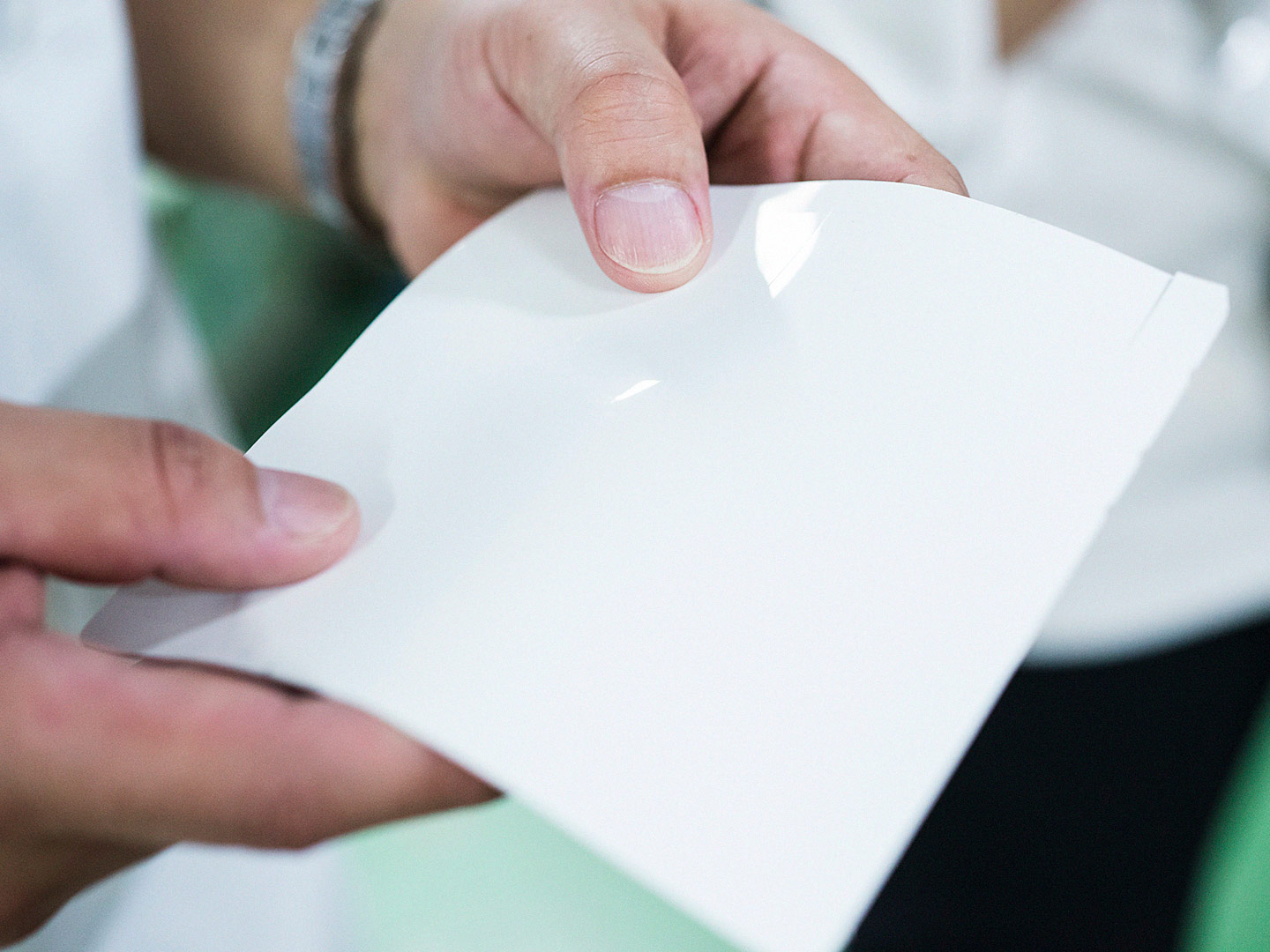
Fukakusa: The blended material is like a paint, and we make it into a kind of skin. It’s a high-viscosity, paint-like material, and we flatten it out and cook the excess solvent out of it as it flows slowly past, until it’s a flat sheet like this. Doesn’t it look like a rubber sheet?
I certainly remember the jingling sound from the white panel in the video, but more than that, I noticed the suppleness and thinness of it. What’s next in the process after the solvent is cooked off?
Fukakusa: After we cut the sheet to the width of the product it’s for, we set it in a metal molding mechanism and stamp holes in it. Can you see the holes?
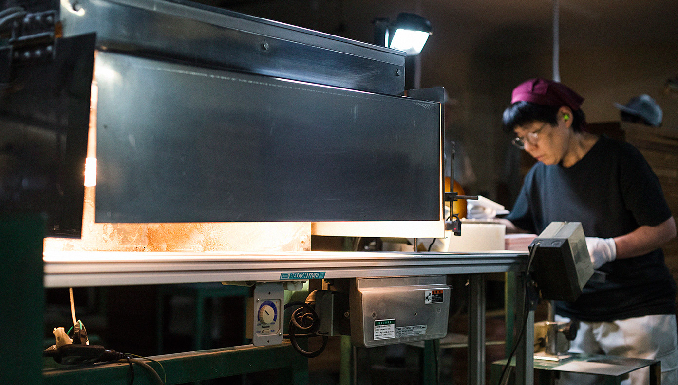
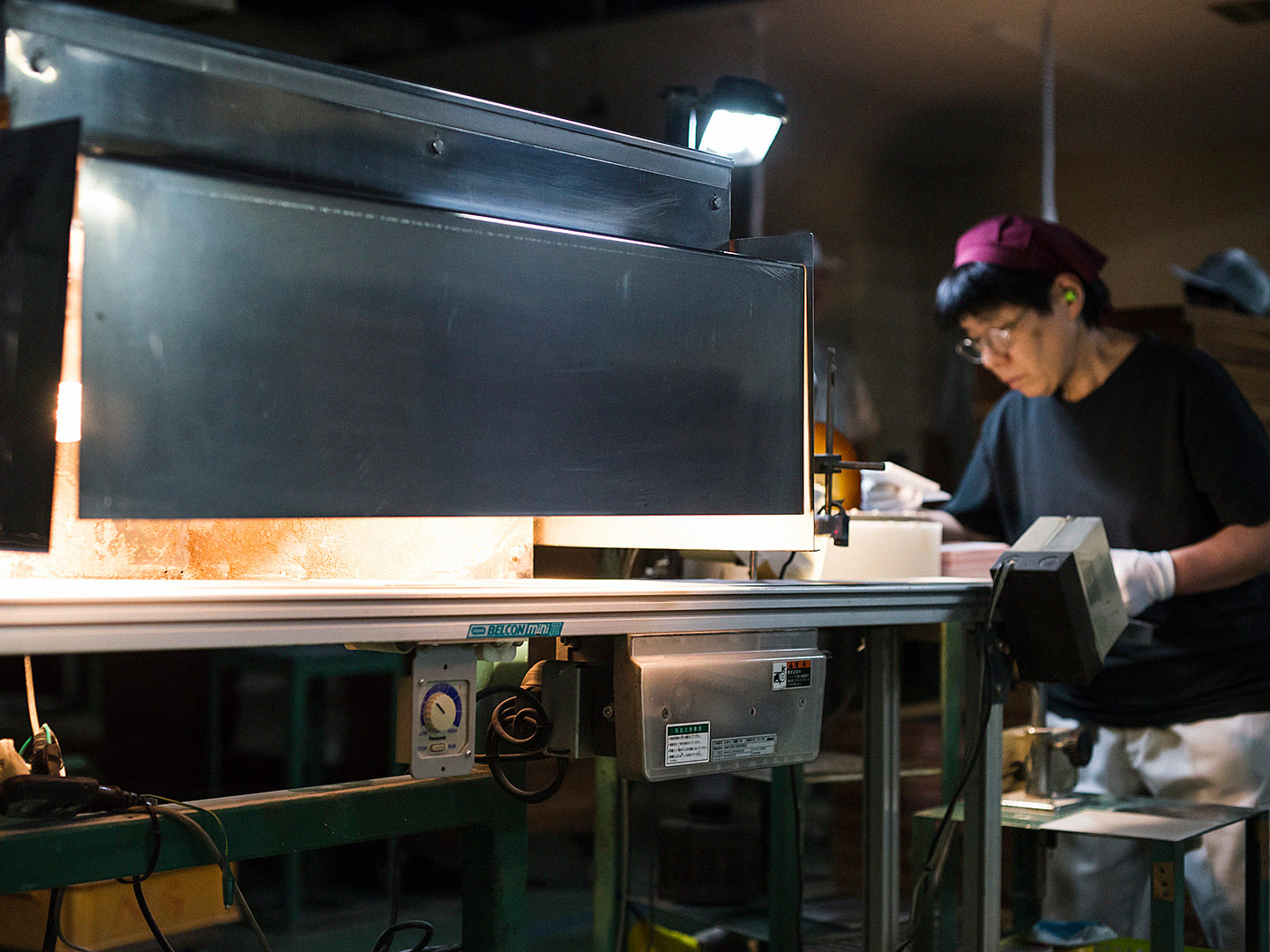
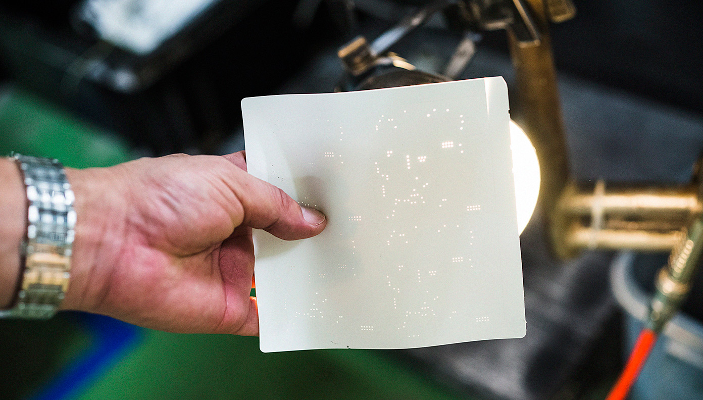
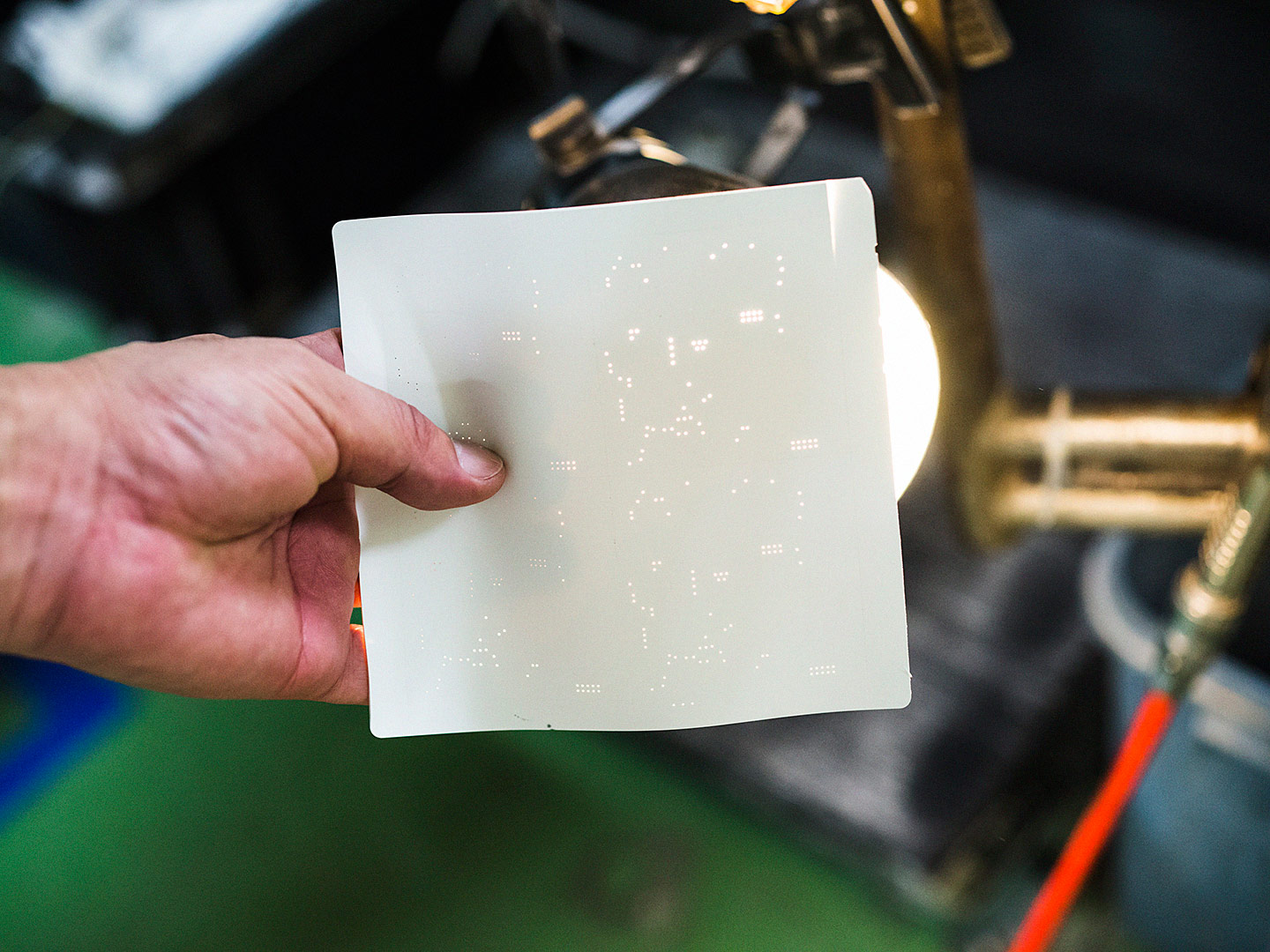
Then you look closely you can see there are a lot of holes in it. Small enough that you have to look through it to see them. They look vaguely like electric circuits.
Fukakusa: That’s right, we’re going to print electric circuits to match these holes. We put these holes in the sheet before we fire it, while it’s still soft. Then we fire it for a long time in a specialized kiln at between 1500 and 1600 degrees Celsius.
I see. So it really is “ceramic” in the pottery sense.
Fukakusa: Exactly. It requires the knowledge and techniques for blending and firing ceramics.
Now that I see the connection between ceramics manufacturing and electrical panels, it doesn’t seem like such a leap. However, don’t electrical devices have their own unique difficulties compared to ceramics?
Fukakusa: We make electrical parts, so they have to have mechanical accuracy, but the manufacturing process still has some quite analog aspects. Along the way from blending the raw materials to firing the product, there are all sorts of variables. For example, since we use natural raw materials there may already be variation from the start of the process. The exact same product might vary in measurement once you fire it, or it may crack a little bit, etc. It’s similar to baking a cookie (laughs). So we do preliminary testing before the manufacturing process gets properly underway.
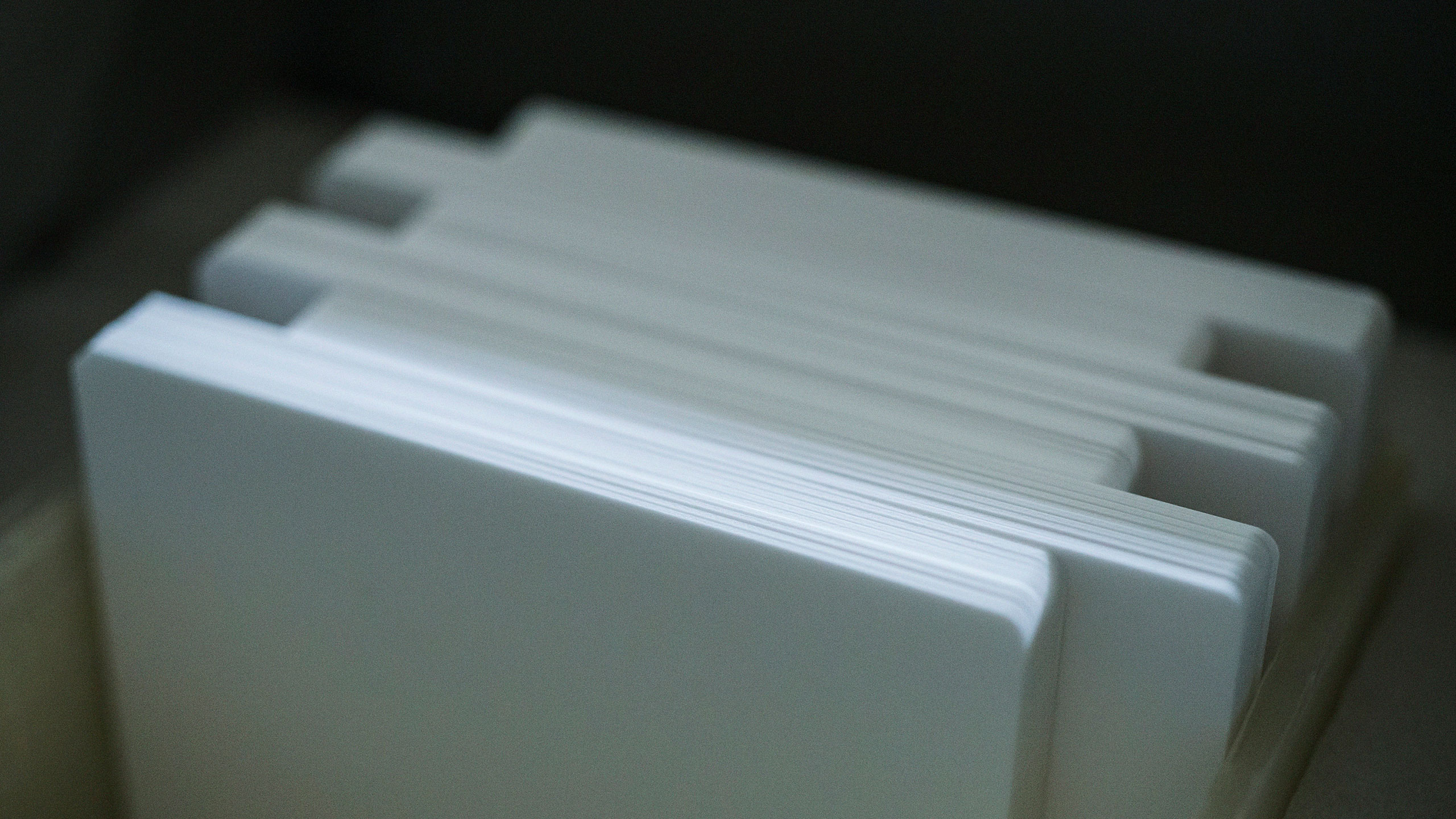
“Artisanship” is usually taken to mean that the product varies according to who’s making it, but it’s important that there be no variation in our products.
The subtle adjustments needed for each different material seem difficult. I wonder whether there is also an element of artisanship involved?
Nakamura: For example, you have to adjust the depth when you stamp holes in the sheet while it’s in the metal mold. You have to adjust the settings of the machine depending on the sheet material, the thickness of the sheet, etc. There’s no instruction manual for operating the blade that cuts the width of the sheet. Even though there are guides drawn on it, you can’t know the best setting without a lot of experience. However, you also don’t want it to get too artisinal.
It’s the same for blending the material. Different materials mix differently, but when you have less experience you tend to just mix them however. And sometimes you do it better, and other times it doesn’t turn out like you wanted. That’s when having an experienced veteran can make a difference. And if you do things according to their experience and advice, you can make a good product.
But even though “artisanship” is usually taken to mean that the product varies according to who’s making it, I think it’s important that there be no variation in our products. A factory where the processing line can’t produce a consistent product without the presence of an artisan is not a good factory. Of course there might be differences in experience or technique, but that’s at the research and preparation level. For the actual manufacturing, you have to work out ahead of time the subtle adjustments required to always produce a consistent product.
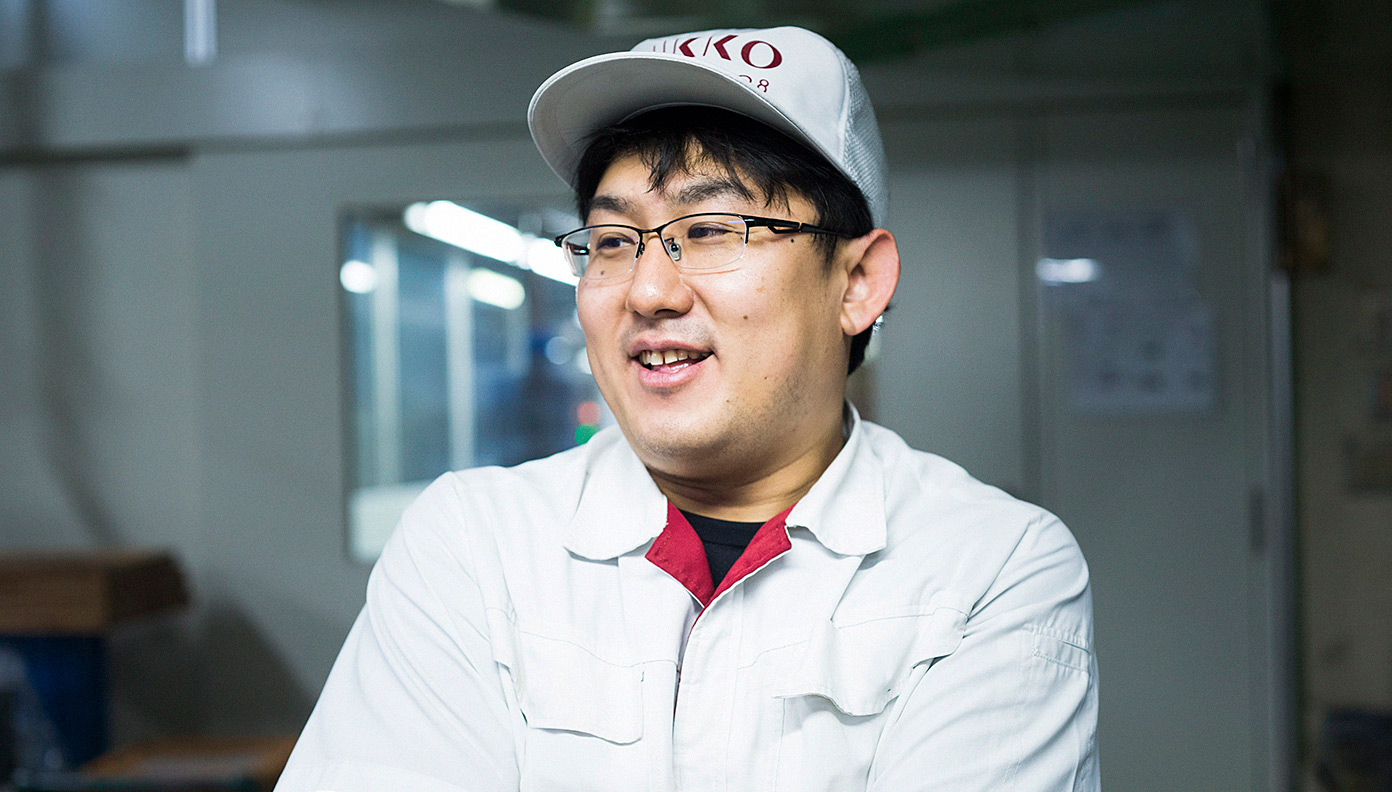
The video also has a scene where they cut the panel using a laser.
Nakamura: They’re not cutting it. They’re punching tiny holes in the panel after it’s been fired. Basically it’s a perforation. The laser perforates it, and then someone separates it manually.
A moment ago you put holes in it in a metal mold before firing it, but in this case the holes go in after it’s been fired. How are these cases different?
Nakamura: When I mentioned a moment ago that there can be slight variations in the fired product, I meant that there can be differences in the measurements of the product depending on whether it’s cut before firing or after firing. Even with material where size only varies by less than a tenth of one percent, the bigger the product is, the bigger the size variation can be. On the other hand, a laser can cut to the exact specs of the design, so the measurements will be accurate. So we cut the larger products with a laser after firing. We decide whether to cut first or fire first depending on the size of the product.
I’ve used a laser cutter before, but it was to make a complete cut. Is there some reason that you leave the actual separation to be done manually?
Fukakusa: It’s really just for the sake of efficiency. It takes time to cut completely with a laser. More than twice as long, actually. It’s simpler to perforate it and separate it manually. We use our own handmade tool to separate it.
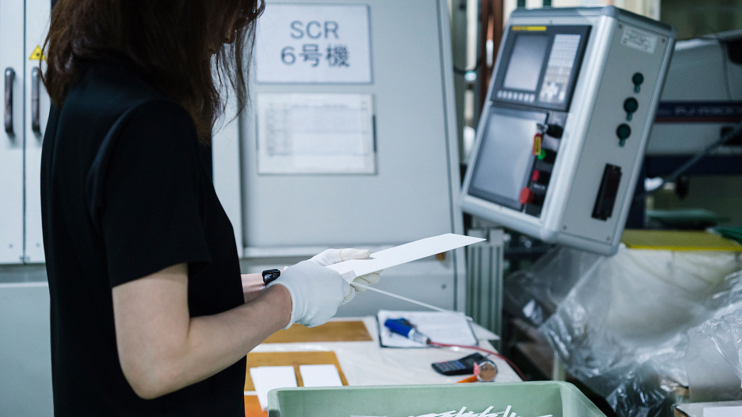
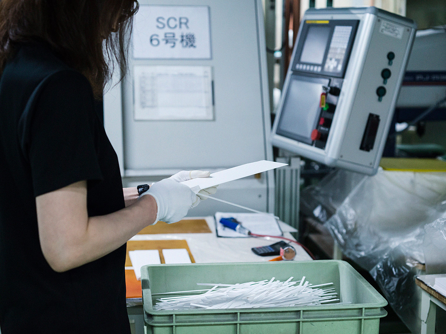
Printing electrical circuits is like printing a very fine, very complicated silkscreen.
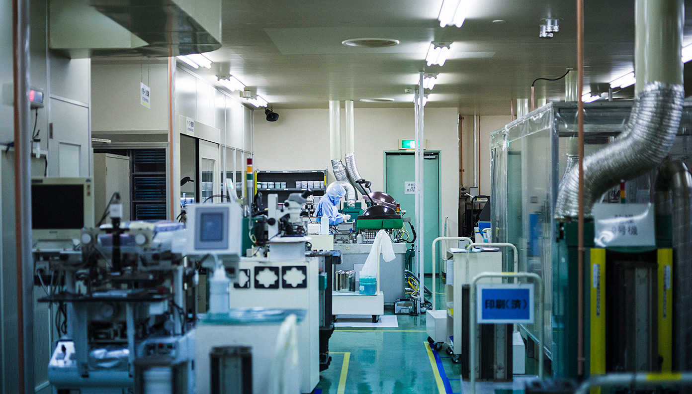
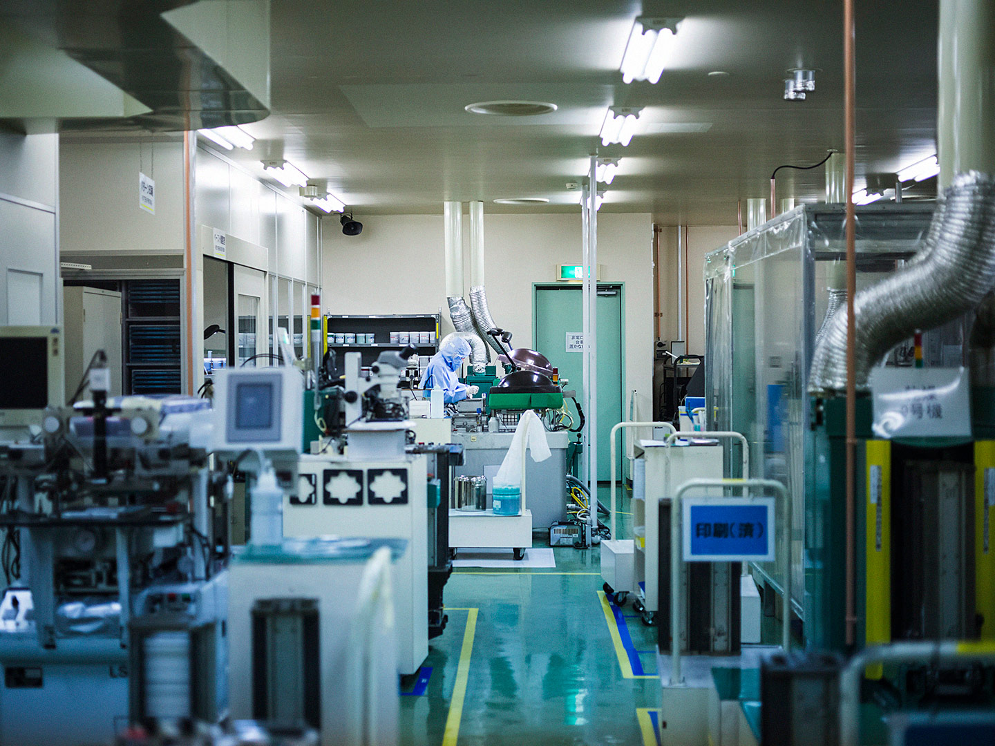
Fukakusa: Once it’s been fired, the next step is printing the circuit. We have a clean room where we make the circuit panels. Normally only authorized personnel can enter. Only special guests have ever seen it.
Since you use a clean room, that must mean everything has to be very sanitary, right? Like you have to wash your hands, etc.?
Fukakusa: We’ve never cleaned it (laughs). Really it just means avoiding dust or debris. Tiny contaminants are the natural enemy of electrical circuits. So we wear special suits, and we pass through a machine that blows off any dust or debris before we enter the room.
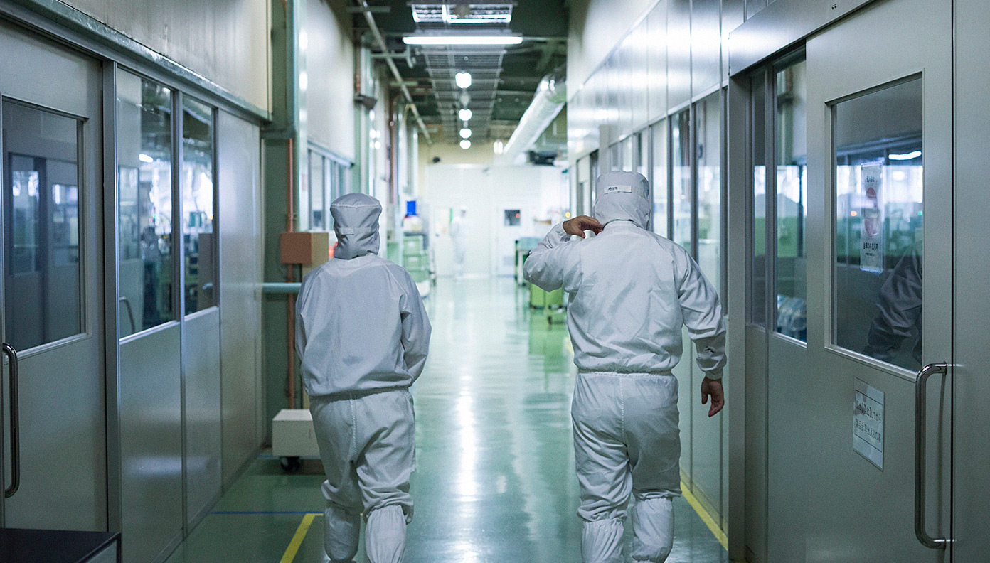
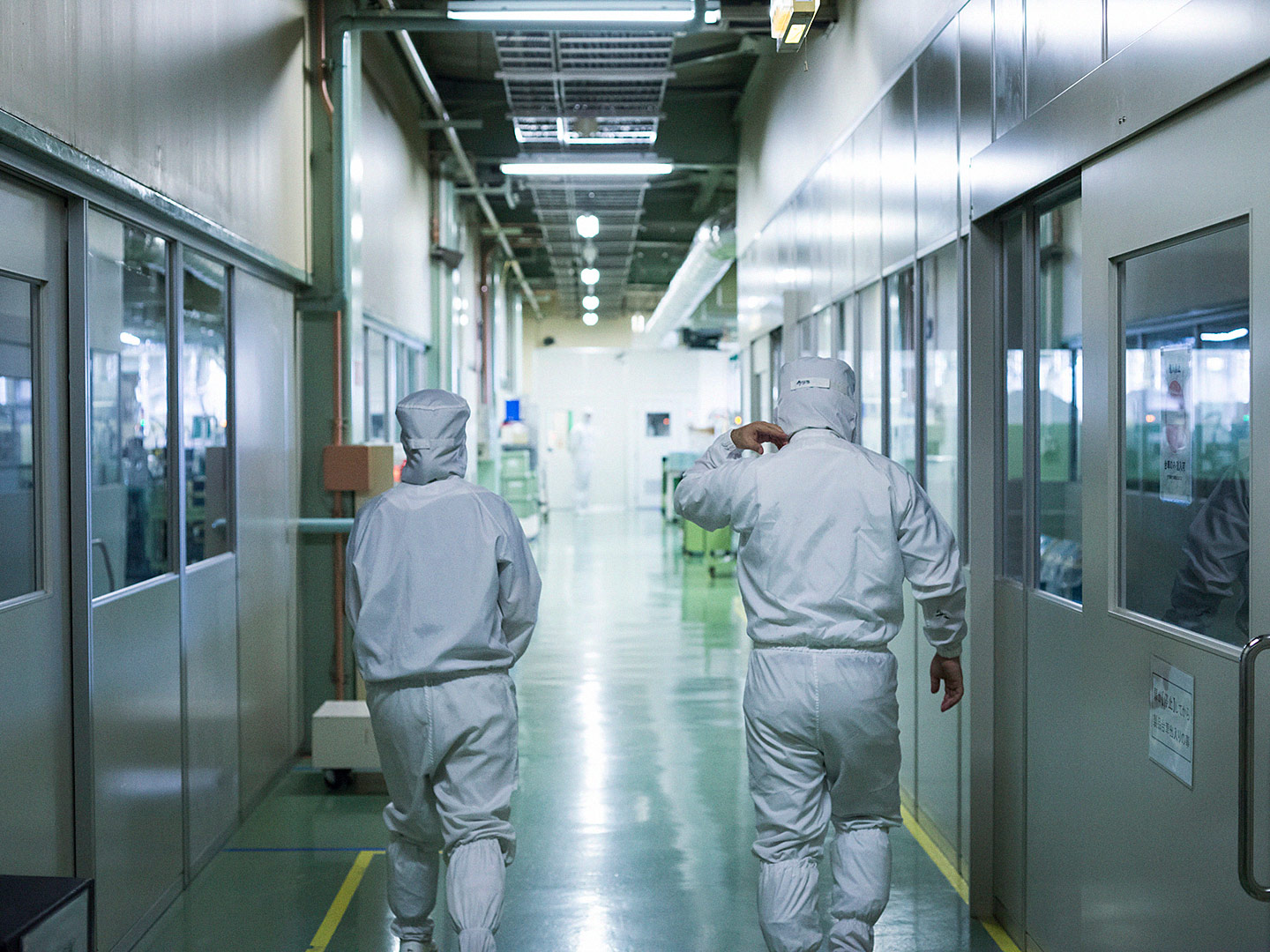
How do you print the electrical circuits?
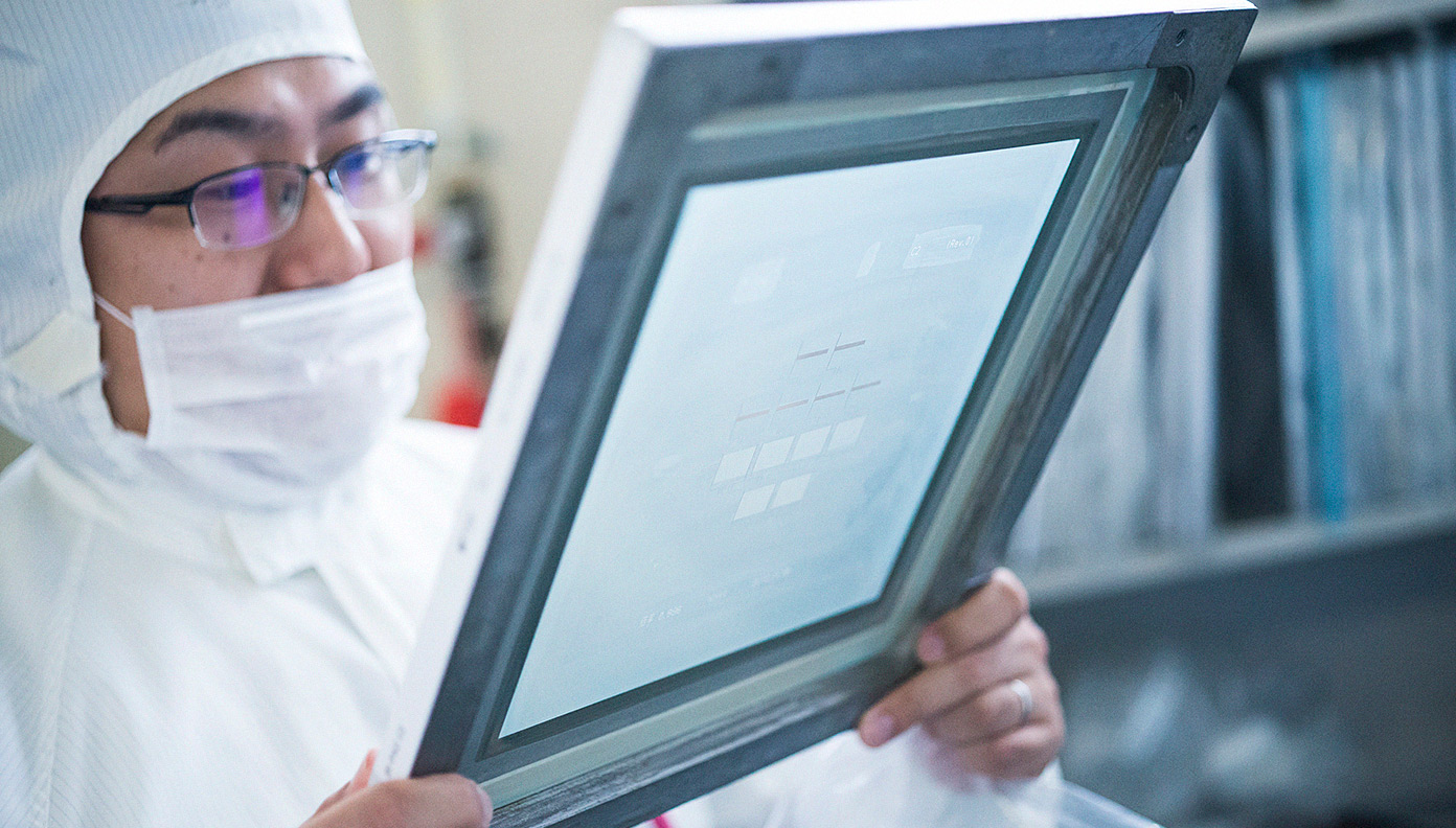
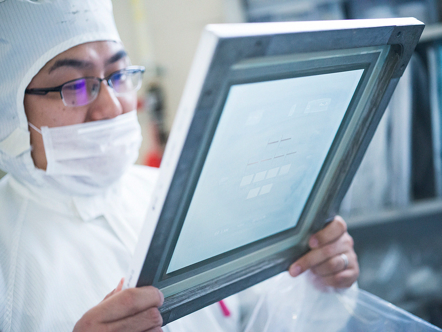
Nakamura: We have a template for printing electrical circuits. We take the ceramic panel you saw earlier, place a template like this on top of it, and print fine metal lines through it onto the panel.
Is it basically like using a silkscreen to print a t-shirt?
Nakamura: You can picture it like a very fine, very complicated silkscreen. The circuit patterns are different on the front and the back. We fill in the holes with electrode material, and make it so that electricity entering through the front passes through to the back. Of course I’m sure that other companies have a similar manufacturing process. Each company uses its own kind of material, and we use our original electrode material. The electrical resistance varies from material to material. And by the way, it’s not just the electrodes. The cover glass material that protects the electrodes also has a front and back.
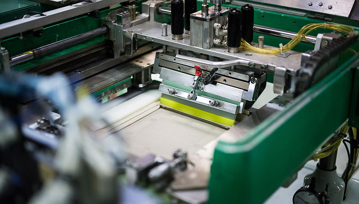
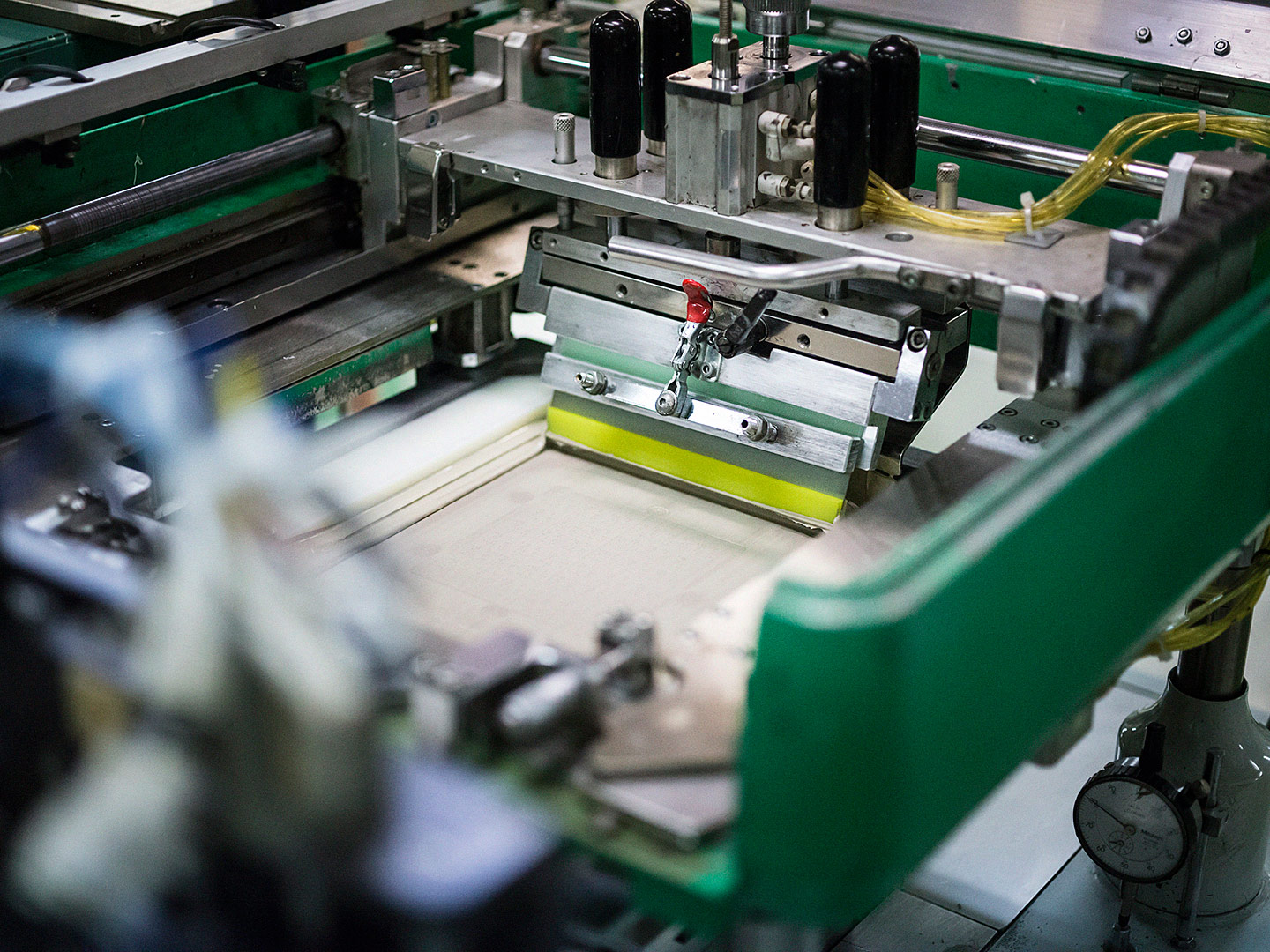
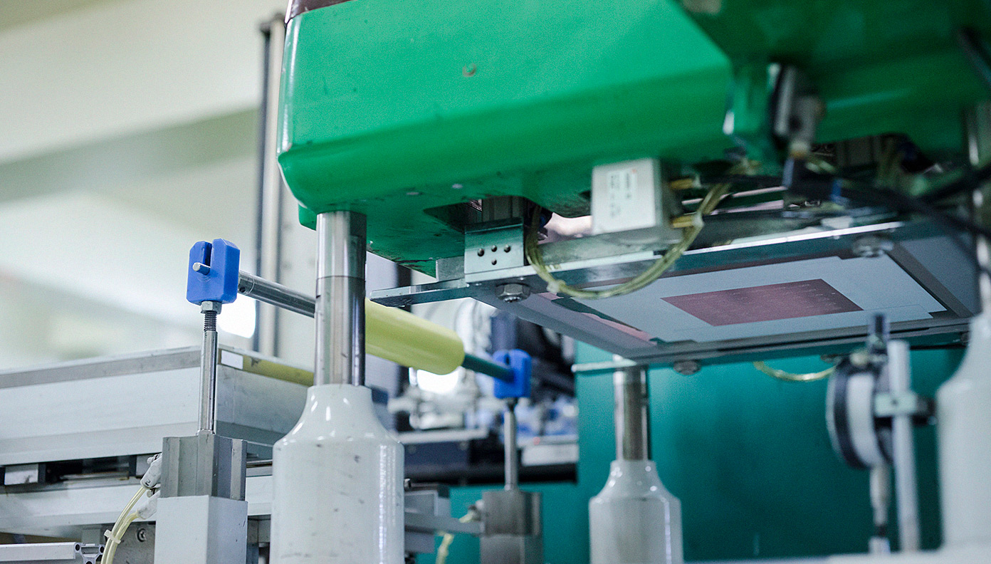
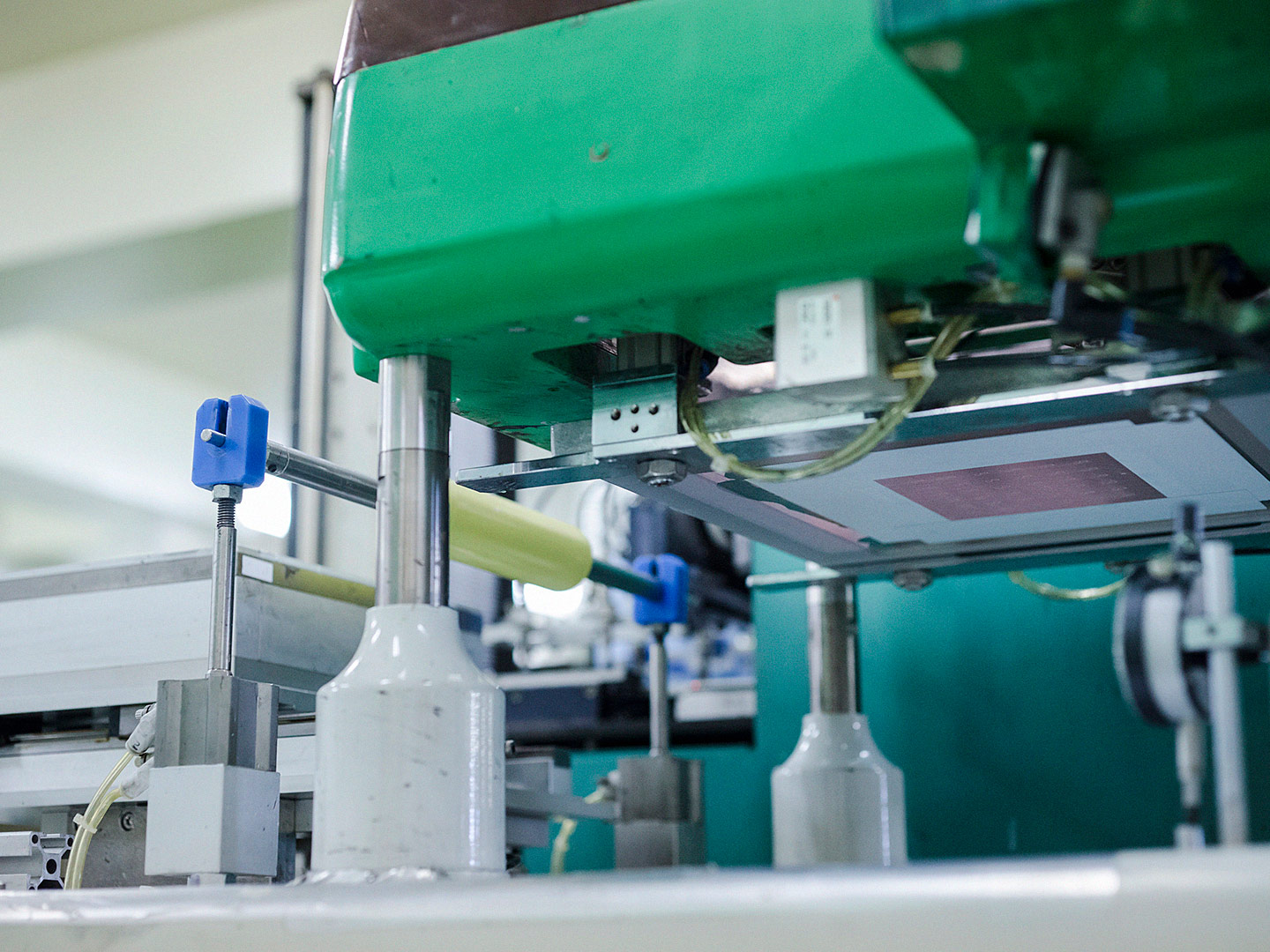
Ceramics-firing techniques and picture printing techniques: these two things make up the core of Nikko’s unique craftsmanship.
Do your manufacturing clients ever have specific orders for specific circuit layouts?
Kanda: That happens a lot. They send us design diagrams with specific sizes or circuit patterns. The design digrams don’t say anything about manufacturing method, so we do the job of figuring out the “recipe” of what machine to use and how to make it when we actually manufacture it. That’s fine if we’re able to manufacture it to match the design diagram, but sometimes we can’t. In cases like that, we might suggest adjustments in the design, like the spacing between the circuit lines or how they’re arranged.
So sometimes orders do come in that are difficult to execute.
Kanda: That’s right. We also do multiple tests while adjusting the machine’s processing conditions and settings little by little to see how we can make it. Sometimes we can just improve upon something we’ve made before, but other times we have to start from scratch. There are times when it just doesn’t turn out how we want it, or it doesn’t go well. Particularly when the raw material changes, it often doesn’t work. In those cases our materials team and our manufacturing process team might work together to figure it out through trial and error.
What do you find to be difficult when you’re doing repeated test runs?
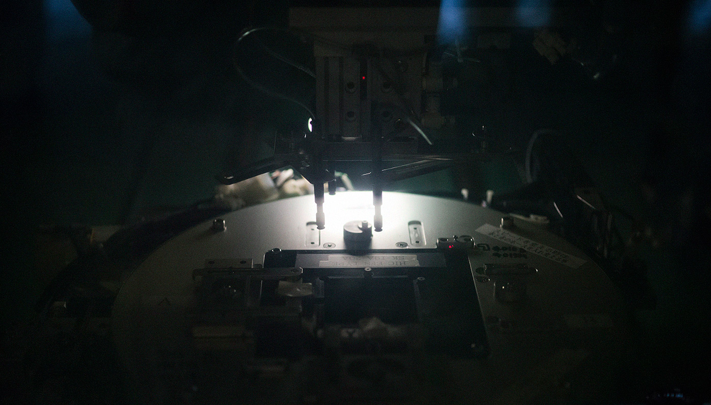
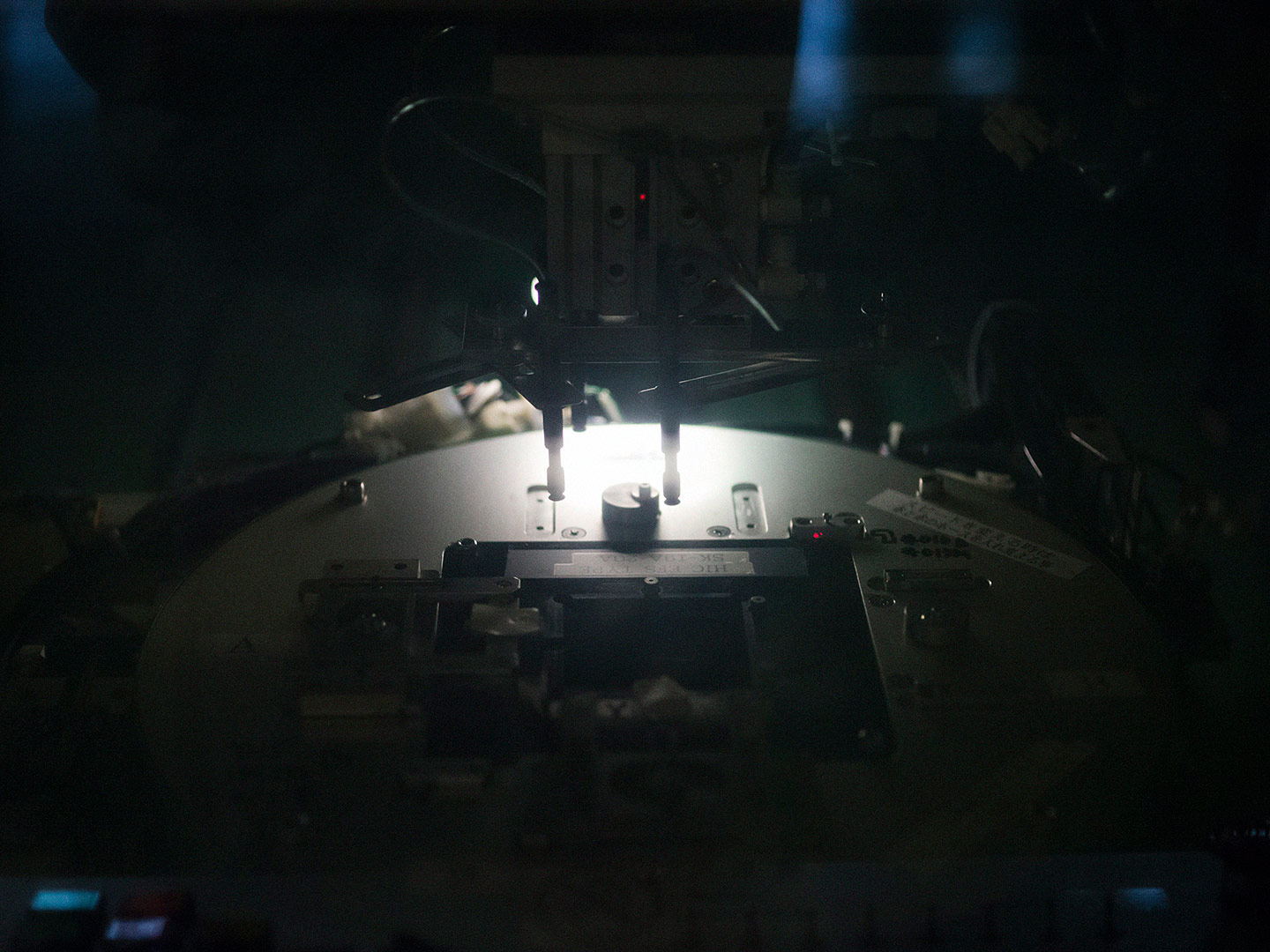
Kanda: Calibrating the machine is super hard! Sometimes you have to calibrate the circuit pattern printing down to a single micron. My experience working at that level is still very much lacking so it’s hard for me, but then one of the veteran workers will come and fix it easily. It’s like the machine is a part of them.
A single micron?! You’d need a microscope. When is that kind of calibration necessary?
Kanda: We make fine adjustments to the thickness of the circuits. Electricity has to pass through them, and the resistance goes down when they’re thicker. Imagine a water pipe. When it’s big a lot of water flows through it, and when it’s small, not much water can flow. It’s the same as that. There’s a standard maximum resistance value that we are required to maintain in all our circuits.
I was thinking they look so detailed and complex, but you can’t tell a single micron of difference just by looking at it.
Kanda: Actually it’s complex in more ways than just the thickness, and you can’t finish with just one imprinting. You use multiple templates in sequence, and imprint many times. You dry and fire the product you just imprinted, then you imprint the next template, and you repeat that process until you finish with one last firing. This same imprinting technique is actually also used in making ceramics.
So actually you’re applying ceramics-making techniques in a number of areas. Is that what makes Nikko’s manufacturing unique?
Fukakusa: I think maybe you can put it that way. Nikko started with techniques for making dishware. When you put pictures on dishware you might paint them by hand, but things like floral patterns are often printed on. The artisan prints the picture on a transfer sheet, sticks it to the dishware, and fires it again. The sheet contains a substance which transfers the color of the picture, so when you fire it the paper burns away leaving only the pigment on the dish. And the shade of the color varies depending on the firing temperature. Techniques for firing ceramics, and techniques for printing pictures on them. These two techniques were the background we needed to start manufacturing circuit panels. This might make us quite unique in the world.
FACTORY
nikko
NIKKO Company
Founded in 1908. The Nikko factory is located in the town of Hakusan in Ishikawa Prefecture, Japan. Nikko started in the Meiji era as a manufacturer of ceramic dishware. Today the company manufactures what are known as “functional ceramics,” such as electrical circuits and fiberglass reinforced polyester resin (FRP), for use in household electronics.Using ceramic-making techniques, manufactures cutting-edge circuit boards that are essential to automobiles and smartphones.
Headquarters/Hakusan Factory located at 383 Ainokimachi in Hakusan, Ishikawa, Japan
